Introduction
As I've explained in part 1.5, I've had quite some issues in the beginning of the project. However I was able to design adapter boards for the display, buttons and the rotary encoder. They also required multiple revisions, but nevertheless they are now done and they are enough for me to proceed with the project. I've had a lot of issues while trying to make the buttons work well, but I think I've got the hang of it now. The display on the other hand is working nicely from the start and I will do further development in the final part. I've tried to make the adapter boards as generic as possible so that I can actually reuse them in some other projects or prototypes.
Display
Schematic
I've made a minimalistic adapter board for the RX12864H-BIW display from Raystar. I like this specific display since the it's quite cheap, compact and easy to use. This exact display uses the ST7567 driver and requires only two small external caps and basically nothing else. The downside is the FFC connector and a requirement for quite tricky mounting holes (also it's always out of stock at TME). I've also included smd solder blob type switches on the board for all the pull-ups and pull-downs that my project requires (hardwiring is bad) and finally a MOSFET for driving the backlight with a PWM signal. The schematic in all it's simplicity is shown below.
 |
| Adapter board for the RX12864H display from Raystar |
The PSB, ERD and RWR connections are designed for the serial configuration that I'm going to use. These are specified in the datasheet. For the backlight resistors R2-R5 are connected in parallel, because a single 0603 resistor cannot handle such power that is going to be dissipated there (approx. 100 mA * 1.5 V = 150 mW). Typical power rating for an 0603 resistor is 1/16 which is 0.0625 W, so it's a good idea to split the current to at least three resistors. It would make much more sense to use a larger resistor but I only have a good selection of 0603 resistors. SW1 is also there for bypassing the backlight control in case it's not needed.
The only issue with this board is that the backlight will easily flicker if the input voltage varies even slightly. This happens especially in the device I am building since the current consumption of the ESP32 changes quite wildly. I've seen this issue in some previous project (while using ESP8266), but have forgotten it until now. Adding capacitors doesn't really help but adding a voltage regulator is an adequate filtering solution. The 3V3 is unfortunately not enough for the backlight since the forward voltage is 3.3-3.7V. For this reason I've decided to add an adjustable regulator and set it to 4V in the final design. The voltage drop of the regulator should be small enough for the device to work even with 4.5V input voltage (for very bad cables / power supplies). I was too lazy to make a new revision of the adapter with this regulator included, but perhaps some day I will. A good choice for an adjustable regulator is AP2127K-ADJ which is in a SOT23-5 case, can handle current up to 400 mA and has a small voltage drop. Additionally datasheet of the regulator has exact resistor values calculated for 4 V output. :)
The display is intended to be connected with the SPI interface. In addition to the standard SPI interface (Clock, Data In & Chip Select), the display uses typical D/C-signal (Data/Command, although it's marked A0 which probably means Address) and a reset signal. All this can be seen later from the final design.
PCB
I've made the PCB only slightly larger than the display. Only so that the mounting holes, connector and pin descriptions can fit on the board. This time I also remembered to include as much useful information as possible, for example the name of the driver chip, suggested resistor values, SDA/SCL mapping and C1/C2 voltage ratings (on the bottom, so not seen here). Also the FFC connector and smd solder blob type switches are on the bottom side. The top side of the PCB is shown below.
 |
| Adapter board for the RX12864H display from Raystar |
The trickiest part was to do the mounting holes for the display module. There are four different details here. The largest hole (shown in grey) in the middle is for the flex cable. The flex happens to be so long that it can be folded under the display, through the hole and into the connector that is FPC1 in the middle of the board (on bottom side). Next there are two rectangles on both sides, these are for plastic clips that are used to attach the display to the PCB. Next are the two large through hole pads at the bottom of the display, these are actually for very narrow strips of double sided PCB that houses the backlight (6 LEDs and 6 series resistors). As a side note the max rated current for the backlight is 96 mA, which means 16 mA per LED, which is reasonably conservative. Lastly there are two small mounting holes in both bottom corners of the display, these are only 0.6 mm in diameter and 78 mm apart. Luckily my measurements were correct and JLCPCB was able to deliver the necessary accuracy that the display fits perfectly (at least two test units).
ps. The reason why a second revision of this board had to be made was that I simply didn't notice the small guide pins at the bottom of the display. Additionally I made the through hole pads too large and I honestly don't know why I did that mistake. I also forgot to add multiple resistors in parallel for the backlight, but that was not a big deal for a prototype.
Code
As already mentioned the display is connected with the SPI interface and pretty much imitates the HD44780 interface. There are a few things no note here however. First of all, this is a graphical display, so there is no hardcoded font data. Secondly the data is arranged vertically on the display unlike it is in many other displays. Lastly the datasheet (or any page on the whole internet) doesn't have any clear example on how to use this exact display. However after looking closely at the datasheet, I found all the necessary details and improvised the rest. I did take some pointers from this source, but I'm highly allergic to that level of code.
After configuring the SPI bus, the software should configure the display. The datasheet tells us that the bias should be 1/9. After that the boost level, regulation ratio and EV (?) should be set. Since the input voltage of the display is 3.3V and the typical voltage for the LCD panel is supposed to be 10V according to the datasheet, I've selected the boost level to be 4X, which would result in max voltage of 13.2V. I then selected the regulation ratio to be 6.0 so that the 10V is in the middle of EV setting (based purely on the graph in the datasheet). Lastly I've set the EV value to be 32 which is in the middle of the configuration range. After some trial and error, I've selected the perfect EV value to be 23, but that will vary from display to display. Additionally I've set the Y axis to be inverted, since the whole panel seems to be upside down and I didn't want to invert all the font data. The configuration process is shown below.
void rx12864h_configure() {rx12864h_cmd(RX12864H_BIAS_SEL | 0); // BS=0 -> 1/9
rx12864h_cmd(RX12864H_START_LINE | 0); // Start line: 0
rx12864h_cmd(RX12864H_SEG_DIR | 0); // MX=0 -> X normal
rx12864h_cmd(RX12864H_COM_DIR | (1<<3)); // MY=1 -> Y inverted
rx12864h_cmd(RX12864H_REG_RAT | 0b110); // Regulation Ratio
rx12864h_cmd(RX12864H_SET_EV);
rx12864h_cmd(0x17); // 0..63
rx12864h_cmd(RX12864H_SET_BOOST);
rx12864h_cmd(0b00); // 00=4X, 01=5X, 10=6X
rx12864h_cmd(RX12864H_PWR_CTRL | 0b111); // VB=1 VR=1 VF=1
rx12864h_cmd(RX12864H_DISPLAY_ON | 1); // Display on
}
After the configuration of the display the picture data can simply be sent to the display one 8-bit column at a time. Unfortunately the counters don't wrap, so they have to be incremented/reset manually. The whole update method is represented below. Since the display is 128 x 64 pixels and has a vertical configuration, there are exactly 128 columns and 8 "pages". The data is sent in bursts of 128 bytes, so one "page" at a time (as a single transmission event).
void rx12864h_update_display(char *picture) {
for(uint8_t i = 0; i < 8; i++) {
rx12864h_cmd(RX12864H_PAGE_ADDR | i);
rx12864h_cmd(RX12864H_COL_ADDR);
rx12864h_cmd(0x00); // Clear column counter
rx12864h_data_burst(picture, 128);
picture += 128;
}
}
Lastly there is the backlight. "Fortunately" configuration of PWM is "very simple" in ESP32. I use lot's of quotes, because I can see how it's made "more simple" for the end user and somehow it's still more complicated than in an AVR. Anyhow, I've configured one pin to output an 8-bit PWM signal with the frequency of 1 kHz and that seems to work just fine to control the backlight. I will not share an example here, because it can easily be replicated from here (also it's just ugly boiler plate code).
Buttons
Schematic
I've made a minimalistic adapter for two buttons and one rotary encoder. Except it's not so minimalistic since the board accepts two different types of buttons and two different types of rotary encoders. The buttons are completely different (D6R90 from C&K and B3FS-4002 from OMRON), but the rotary encoders (specifically EC11J15 and EC11E15 from ALPS) are basically the same except for the mounting (surface mount and through hole). I've wanted to include these two specific button types since they both are very good in quality but differ quite much in the height. If I were ever to design a case for this device, the D6R90 would look quite nice poking from the enclosure by itself (as I've done previously in some other project, albeit with cheaper buttons).
Additionally there are pull-ups and debounce filters on the board. Unfortunately the pull-ups are done incorrectly on this board, since the pull-up resistor is on the wrong side of the series resistor. This means that the resistors work as a voltage divider when the button is pressed, which is okay if the values are chosen correctly. However this means that the rise time of the button signal is significantly longer than the fall time. Additionally the rotary encoder has a minimum working current of 1 mA (as stated in the datasheet), which limits the pull-up resistors to 3.3 k when the used voltage is 3.3 V. Apparently the using the rotary encoder with a smaller current will introduce much more noise as was stated in some source, which I unfortunately no longer have, sorry. The schematic is shown below.
 |
| Adaptor boards for D6/B3FS series buttons and EC11 series rotary encoder |
As can be seen in the schematic, the two button types and rotary encoders are connected in parallel, since only one of these can be soldered at a time.
PCB
The PCB is equally simple in this case, the different buttons and the different rotary encoders are located on top of each other so that only one type can be soldered at a time. This was quite simple and logical thing to do in my opinion. The board is shown below in all its glory. I didn't even bother adding a ground plane and I probably should, since the boards look very odd without a ground plane.
 |
| Adaptor boards for D6/B3FS series buttons and EC11 series rotary encoder |
The only issue with this current board itself is that I forgot to relocate the SW5 and SW7 labels. :(
ps. The reason why the second revision of this board had to be made was that I used ready made components in the first revision and the symbol for the B3FS had wrong pinout, which means that the button was constantly shorted. Also the EC11J15 did not fit in it's footrpint. You might ask how an SMD component cannot fit into its footprint that was supposedly made by the manufacturer and I simply do not have an answer for that. I only know that it physically did not fit, since the tap at the bottom of the component did not fit into the hole in the board. Moral of the story, never use ready made components. If you want something done, do it yourself.
Software
The buttons are very simple devices. I mean they should be. However I've spent quite some time trying to make them work properly with the ESP32. I suppose the source of these issues is that I tried to use GPIO interrupts to read the buttons as I've done with many AVR projects previously. It seems that compared to an AVR, the ESP32 is much too sensitive for detecting the falling edge. I suppose I could have used detection of the rising edge but then the schematic would need to be changed and that's just stupid. I've spent many hours trying to make this work using interrupts, but then it took only a few minutes to make it work after I gave up on the interrupts.
Reading the properly debounced buttons without an interrupt is very simple, especially when using FreeRTOS. You basically make an endless loop with a delay statement, that checks the state of the button pins and compares to the previous state. This way a falling edge can be detected, which means that the button has been pressed. Fancier features like the long press support can be added later of course, but edge detection is the basic principle for reading a button press.
The rotary encoder is a bit more difficult. There are two pins in this encoder and they are shorted in specific order when the encoder is turned. The specific order is gray code (not binary) for good reasons. However we don't really need to care about that, we just define the four states that can be created with two pins, and try to detect specific state changes. The principle is basically the same as with the buttons, but here we check the state of multiple pins instead of just one. The state change is then interpreted as one clockwise or counterclockwise step. Below is a picture that shows the four stages of a rotary encoder (taken from the ALPS datasheet).
 |
| Gray code of a rotary encoder |
Let's assume that the left dotted line is at state 0 and the right one is at state 2. In this case we can, for example, detect state changes from 0 to 1 and from 2 to 3 as one clockwise step. Similarly a change from 3 to 2 and from 1 to 0 would mean one counterclockwise step. And that's basically it. Below are first some example definitions for pins and rotary encoder states. The states are defined similarly to the picture starting from the left dotted line.
#define KNOB_RE_A_PIN 27#define KNOB_RE_B_PIN 26
#define KNOB_BUTTON_PIN 14
#define RE_MASK ((1ULL<<KNOB_RE_A_PIN)|(1ULL<<KNOB_RE_B_PIN))
#define RE_STATE_0 ((1ULL<<KNOB_RE_A_PIN)|(1ULL<<KNOB_RE_B_PIN))
#define RE_STATE_1 ((1ULL<<KNOB_RE_B_PIN))
#define RE_STATE_2 (0)
#define RE_STATE_3 ((1ULL<<KNOB_RE_A_PIN))
After that we can make a task for reading both the buttons and the rotary encoder. I've also specified defines for each action, since they cannot really match with the pins (at least in case of the rotary encoder). Another remark is that I've used the GPIO_REG_READ macro instead of the usual gpio_get_level simply because there's no need to use the latter one. I suppose the latter one would also have some unnecessary overhead. Lastly the actions are sent to another task with the help of task notifications, which is a great feature by the way. In any case here's the example code.
static void read_buttons_task(void* arg) {uint32_t prev_buttons = 0xffff;
vTaskDelay(10 / portTICK_PERIOD_MS); // 10 ms delay
uint32_t buttons = GPIO_REG_READ(GPIO_IN_REG);
xTaskNotify(gpio_task_h, KNOB_CW_BIT, eSetBits);
if ((prev_buttons & RE_MASK) == RE_STATE_2 &&
xTaskNotify(gpio_task_h, KNOB_CW_BIT, eSetBits);
xTaskNotify(gpio_task_h, KNOB_CCW_BIT, eSetBits);
if ((prev_buttons & RE_MASK) == RE_STATE_3 &&
xTaskNotify(gpio_task_h, KNOB_CCW_BIT, eSetBits);
xTaskNotify(gpio_task_h, KNOB_BUTTON_BIT, eSetBits);
}
SPI Issues
As I've already understood from the start, this project would require something to be able to use multiple SPI devices on the same bus. However I wasn't sure how big of a deal it would be. Originally I might have thought that the SPI library has some thread safety built in, but apparently it doesn't. It actually took me quite a while to understand why the device was crashing when I tried to change the volume. Since the VS1053b chip has a separate control bus, the volume control was clashing with the upload of audio data and thus the device crashed (with a ~50% probability). So I technically had to solve this issue before I even connected the display.
As the warning in the link above states, there are two options for using multiple devices on the same bus. One would be to refactor everything nicely into one task. I didn't want to take this path, since I would like to have the display and audio decoder as separate as possible. The second option is to just use a mutex. This was a much nicer option, even if it might not be as efficient (see background here). (I might actually rethink this later on, especially if I want a high and consistent refresh rate for the display. After all, the common task can be in the main module and only call respective functions from the display & audio decoder modules.)
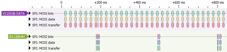
With this info the solution is simple, just create a mutex object in the main module and pass it to both the display and the audio decoder modules. There is still a possibility that for example the volume change will interrupt the update of the display, but it will take a tiny amount of time and it will not crash the device. Previously I wouldn't have known how to measure or debug these kind of things, but luckily I now have a logic analyzer and was able to capture these events. For your viewing pleasure, below is a screenshot from PulseView with decoders added for audio decoder data and display control & data.
 |
| SPI traffic of the audio decoder and the display captured with PulseView |
The SPI frequency is set to 1 MHz in this test, because I have a rather cheap 24 MHz logic analyzer and it's not really usable beyond 2 MHz. Also with 1 MHz it was very easy to capture such a case as seen above. The audio data is sent in bursts of 32 bytes as already explained. For this reason the display update can interrupt audio upload, since there is no priority whatsoever. The display data on the other hand is sent one "page" at a time, which is 128 bytes. Additionally the control data for the LCD (as explained in the software part) can be seen in the picture, since the control and data are sent to one SPI device as seen by the ESP32 (unlike for VS1053b).
Let's do some math here just to measure what kind of performance can be expected from the device. Let's assume that the SPI frequency is 1 MHz and we have an 128 kbps audio stream. A single display update would require 128 * 64 bits of data to be transferred (without any overhead included). We also know the overhead for the control, which is 3 bytes per page so 3*8 bytes in total. With this info we can calculate the (theoretical) maximum refresh rate of the display.
(1 000 000 - 128 * 1024) / (128 * 64 + 3 * 8 * 8) = ~100 Hz
This is some very good performance. Even with 320 kbps stream, the refresh rate would still be ~80 Hz with 1 MHz SPI frequency. We should however consider the unilization of SPI bus, since the ESP32 has also other tasks (even if DMA is used). If we consider 30 Hz refresh rate, the utilization would be (128 * 1024 + 128 * 64 + 3 * 8 * 8) / 1 000 000 = ~14 %. That doesn't really seem much, but we're not taking overhead into account (apart from LCD control). Nor are we taking into account the overhead that comes from the 32 byte bursts for the VS1053b chip. Below is a zoomed out picture of ~1 second timeframe with a 320 kbps stream playing and 3 Hz display refresh rate.
 |
| Zoomed out SPI traffic with 320 kbps stream and 3 Hz display refresh rate |
From the picture it kind of looks that the utilization of the SPI bus is around 50% and it looks like it would be ~100% with the 30 Hz display refresh rate. This is however not a very good analysis since it might look bad simply because of the fancy graphics. Regardless of that we have the option of increasing SPI frequency to significantly reduce bus utilization. The maximum frequency for LCD is 10 MHz and for the audio decoder also 10 MHz, although there is a catch regarding the configuration that I will explain later. With 10x speed increase the device shouldn't have any issues at all. This math is necessary especially if we want to add a spectrum analyzer to the device. And we definitely want to do that later. :)
Result
With the hardware and software shown here, I was able to control the radio and make it display useful information. The first thing to do was obviously volume control and after that followed the menu to control all settings of the VS1053b chip and also change the radio station. The display looks very cool with its blue backlight but it was also quite useful while displaying the buffer usage and the signal strength in real time. The only issue is that the edges of the display look annoyingly bright without any case, as compared to a standard eBay 128x64 LCD with a metal bezel. At least I can say that the picture quality is significantly better.
Also here are the links for display adapter and button adapter EasyEDA projects. It seems that EasyEDA is using some new OSHW Lab platform for sharing projects and I have to say that it looks unfinished. However the EasyEDA project sharing was not that much better so who cares.
Final words
Apart from a few slowdowns, this project is quite on track. I might even be able to finish it before my personal deadline, which is in September.
It's worth noting that while the SMD version of the rotary encoder is quite nice, it's also 2+ times more expensive than the through hole variant at least at LCSC. I wonder why it's like that.


