Introduction
This project actually made me realise that the most important thing isn't what you're doing but it's why you're doing it. I've previously used a very simple ESP32 adaptor board from eBay, the one that only has the place for an ESP32, two buttons, two pull-up resistors, two pin-headers and a text "161015" on it. The reason I used exactly this board is that it doesn't have an integrated regulator circuitry which made it possible for me to accurately measure the current consumption of the ESP32 itself (including a very low current consumption of "deep sleep") without the effect of the voltage regulator. This board however isn't very good and at some point it wasn't very cheap either. For example the board lacks probably the most important thing a board can have, which is the required capacitor (the datasheet recommends 10uF) for the ESP32 module. Since this is a development board, the power is often connected with some random wires. In some cases the resistance of the wires is just too large and the ESP32 starts crashing because of low voltage situations. Additionally the board is large enough to have an usb connector and an optional regulator. Another important thing is the programming connector, which is also related to the previous post.
This is the reason why I decided to make my own adaptor board with blackjack and hookers.. I mean with an optional voltage regulator, USB connector and not one, but two programming connectors. I've also decided to add a stand-by LED, voltage monitoring chip and test-points for the power connections. Obviously all of the components are optional on this board except the ESP32 and the pin-headers. Additionally the original board had all the ESP32 pins connected to pin-headers. I've decided on the other hand to connect only those that can be easily used with the internal flash chip. For some reason I've also decided to make the PCB the same size as the eBay adaptor. I thought that it would be big enough for all the features and eventually it was.
The reason for the first sentence in this intro is that I originally thought I can just add all the features to this board, including the programmer part. Then I realised that I would just recreate the DEVKIT or similar development board. I also quickly realised that the board is simply too small to include all the parts and the programming connector which I really wanted to include. Eventually I realised that it really makes no sense to add everything to the board, since the main thing I want is a minimal development board that would have the programming connector and that I could use to measure the current consumption of the ESP32. For other purposes I could simply use ready made development boards. The USB connector and the integrated regulator is however such a nice feature that I've decided to keep that and simply add a "SMD solder blob" kind of switch. This way it's possible to completely separate the regulator from the ESP32 for accurate measurements. This approach is not as easy to use as a switch, but on the other hand it doesn't need to be "switched" often, it's very compact and has low resistance.
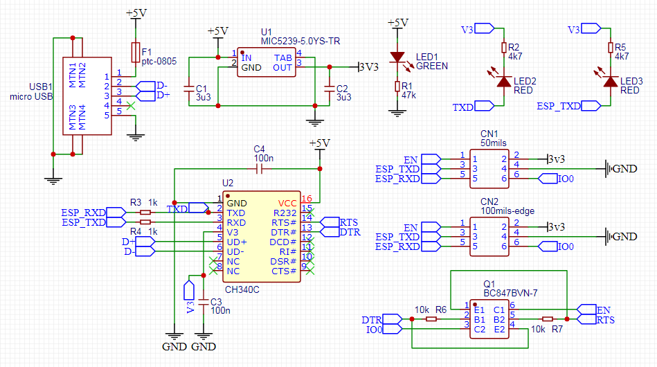
Schematic
The schematic is fairly simple, the main parts are the ESP32 and the pin-headers. Also there are the same two buttons and pull-up resistors, although there is an optional voltage monitoring chip instead of one of the resistors. Then there is the already mentioned USB connector and the voltage regulator. Lastly there are two programming connectors (50mil and 100mil), some test points and the stand-by LED. In reality the connectors could not fit properly on the board, so they are placed so that only one of them can be soldered at a time.

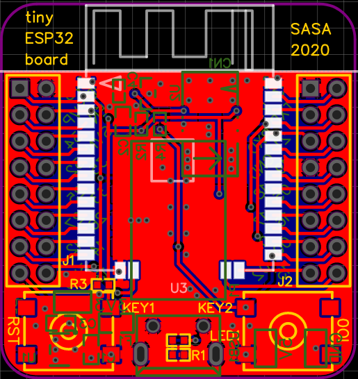
PCB
The board was made to very much mimic the original eBay board. The ESP32 module is on top, two pin-headers on sides and two buttons on the bottom of the board. The stand-by led is between the buttons. The bottom side has the voltage monitoring chip close to the EN pin of the ESP32, two programming connectors pretty much in the middle of the board and the USB port between the buttons. The voltage regulator is located under the left button and the test-points are scattered here and there. The test-points I use can be found from here. I've found them very useful and functional even if they're not very cheap and are a bit difficult to solder properly.
Result
I'm fairly satisfied with the result even though I haven't tested the voltage monitoring circuit yet. I've only used 100mils programming connector and it works nicely with the programmer I've made. Also the "SMD solder blob" -type switch works nicely, but I suppose the gap should be a little smaller. The only downside here is that the LED polarity is not marked as also in the previous project. I should probably do something about that at some point. Also I've used ready-made footprints for the buttons and the silkscreen markings are just huge compared to the buttons themselves. This can be seen from the pictures below. Also there seems to be some manufacturing error with the silkscreen on the top side of the PCB. I have reported this to JLCPCB, but it's not an issue here since this is just a development board and most of the problem is under the ESP32. Unfortunately I did not get any answer from JLCPCB regarding the root cause of the mistake. I was only given options to get new PCBs or get a discount for the next order. The link to public EasyEDA project can again be found here.

Final words
I suppose the only real downside of this project is that I should have done it much earlier. It would have made my life much easier. Luckily it's a hobby and no one's blaming me about it except myself.